Introduction
In the realm of motherboard-level repair, NAND flash replacement and capacity expansion have emerged as mature, chip-level repair solutions designed to address issues such as full storage, performance degradation, or storage corruption. As this chip is responsible for both system and data storage, the repair process necessitates the extraction and migration of data. Skilled technicians typically utilize JCID programmers in conjunction with BGA rework stations to execute the removal, installation, and data writing operations; through precision soldering and low-level data processing, they successfully achieve device storage expansion and system restoration, thereby enhancing the overall performance and lifespan of the device.
Preparing for iPhone NAND Storage Issues and Error Analysis
Proper diagnosis before starting any restore is especially important because NAND-related errors look like motherboard or software problems Common signs include stuck Apple logo, repeated boot loops, iTunes errors, or storage showing incorrect capacity. These problems factor in the direction of a regularly failing iPhone NAND Flash IC, which may even require a replacement or reprogramming rather than a full-board replacement .
Technicians first look at a good concept board under the microscope to check for damage, rust, or signs of previous repairs on the body. A multimeter is used to establish the voltage lines of the NAND field. Clean running conditions are essential, as even minor dirt can affect the high quality of the BGA conversion. Right additionally use the JCID Reader/Writer Programmer to backup any readable data, which allows to extract the necessary gadget records before they are deleted This step ensures secure fact transfer and reduces the risk of continuous data loss during NAND upgrade processes.
Required Tools for iPhone NAND Flash IC Upgrade Process
The fulfillment of a NAND improvement is closely dependent on the quality tools used in the processing process. A professional setup is a hot-air reprocessing station with adjustable temperature control, usually set between 320°C and 380°C for NAND processes Low temperature settings help save your loss to quench of additives on the logic board. A precision soldering iron is also used to clean pads after tile removal.
The most important gear is the AMAOE BGA Reballing Stencil, which ensures perfect solder round alignment during the course of the reballing pattern. High adequate current is carried out before heating, as this improves solder flotation and reduces oxidation of the pad. Microfactor tweezers, antistatic brushes, and PCB holders are required to stabilize the panels. The JCID Reader/Writer Programmer plays a key role in parsing individual NAND information and writing it to a brand new chip, ensuring device compatibility by option Without these tools, successful NAND processing would be extremely difficult.
Safe Disassembly and Logic Board Access Techniques
Proper distance is the muse of a successful NAND restoration. The machine must first be completely switched off, and the display is carefully removed from the use of suction devices and thin plastic options to avoid antagonistic flex cables When the display is complete, the battery is immediately disconnected to prevent a quick circuit at some point during the treatment process. This step is critical to the security and defense of the government.
Next, we will remove the board from the housing using precision screw antistatic tweezers. Technicians should treat the board carefully, especially near the NAND position, which is sensitive to heat and mechanical stress. The hot-air recovery unit is attached to a controlled vent installation to prevent blowing of small connections. In this step, the technician applies electricity around the iPhone NAND Flash IC area, which assembles it for removal. Proper disassembly ensures that the board is still robust to the temporary BGA reworking technique.
Removing and Reballing the iPhone NAND Flash IC Using AMAOE stencil
Removing NAND chips requires controlled heating and precision. The hot air recovery station is about to round 360°C with gentle airflow. The nozzle is placed about three–five cm from the chip to distribute the heat trivially. Once the solder is melted, first-class curved tweezers are used to gently extrude the iPhone NAND Flash IC without using pressure, stopping damage to the motherboard’s pad.
After the table pads are removed, they are cleaned using a lint wick and occasional dust rinse to ensure a flat bottom. The new NAND chip is then outlined using the AMAOE BGA Reballing Stencil, with solder balls placed trivially across the chip base. At some stage of the recirculation, the recirculation is performed to aid solder adhesion. A controlled heating process ensures that all bubbles form the best combinations. This step is one of the most important components of NAND processing, as bad reballing can later lead to boot errors or device instability.
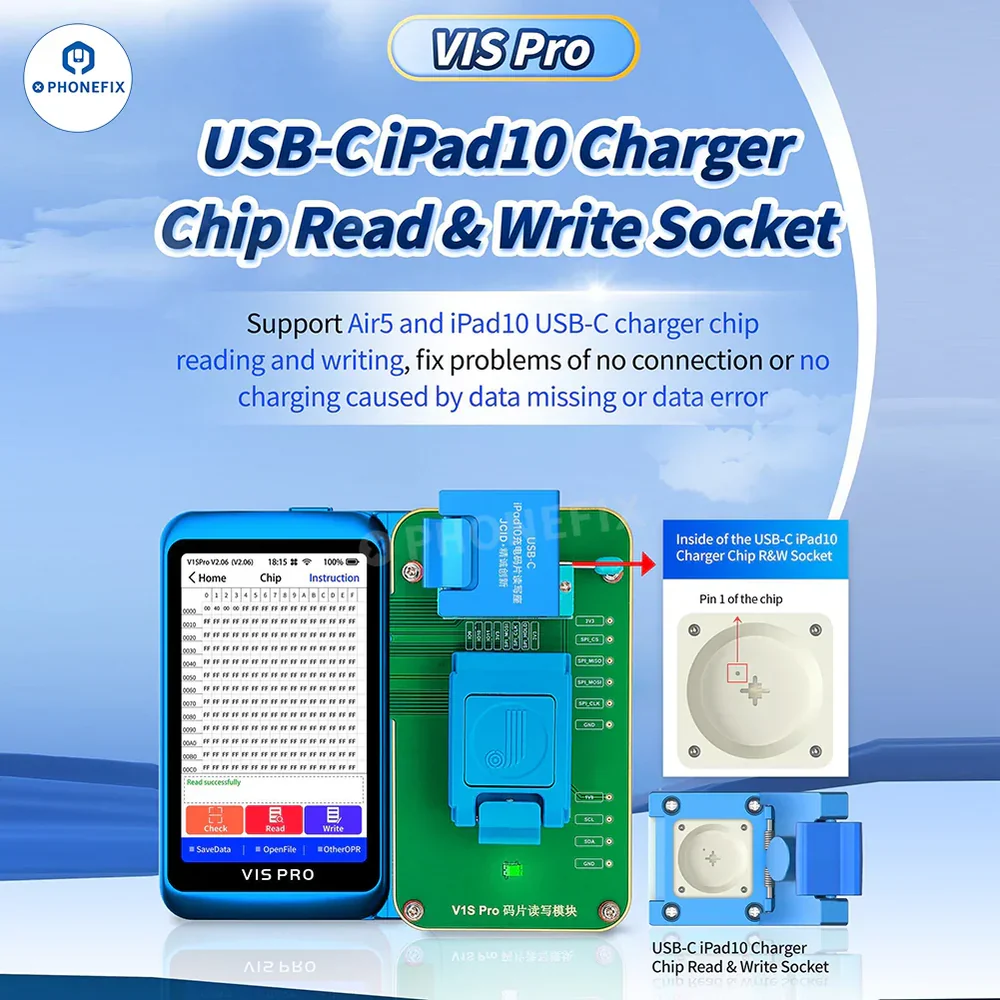
Programming NAND with JCID Reader/Writer Programming and Data Transfer
Once the NAND chip is physically installed, the next step is programming and information transfer. This is where the JCID reader/writer programmer becomes important. The equipment attaches to a NAND chip via a special adapter, allowing technicians to read equipment statistics, serial numbers, and garage configuration from a separate chip or backup file
The programmer is then used to write appropriate firmware and calibration records for the new NAND. This ensures that the iPhone or iPad accepts the advanced garage effectively without activation errors. This method requires careful attention to stay away from disturbing the energy or connection, as this can corrupt the information. Advanced repair shops often use fixed power supplies and software certification kits during writing. This phase is what turns a simple chip choice into a full focused storage improvement that feels seamless to the suspension person.
Reassembly, testing, and verification after inventory updates
After the other programming, the sense table is again carefully assembled back in the engine room. All connectors, including the display, battery reflex, and cables, are securely reattached. The device is then switched on to verify successful starting. If the Apple logo appears and there is a mass of the device at all, it indicates that the iPhone NAND Flash IC update became a hit.
Technicians then check the storage options internal settings to verify that the updated NAND is recognized correctly. Additional stress testing is achieved by installing apps, restarting the device more than once, and checking the balance of smartphones. If any problems appear, it may be necessary to recheck the solder connections or firmware data. Proper testing ensures long-term reliability and verifies that the NAND upgrade method has performed effectively without hidden defects.
Conclusion:
NAND chip replacement and capacity expansion represent an advanced technique within the field of mobile motherboard micro-repair. This process requires a solid understanding of microelectronics and multi-layer PCB structures, and relies on precision equipment to execute data migration and soldering operations. By utilizing tools such as JCID programmers and BGA reballing stencils, technicians can perform flash memory repairs and storage upgrades, thereby reducing the cost of replacing the entire device. This methodology has been widely adopted in the realm of high-end, chip-level repairs; it not only restores device functionality but also extends product lifespans and helps minimize electronic waste.